ftp://78.46.141.148/
check out also for further analysed images http://oms.wmhost.com/misc/
for live discussion join internet relay chat on IRCNet channel #sid
You can get information about the current status of reverse engineering there also.
Content:
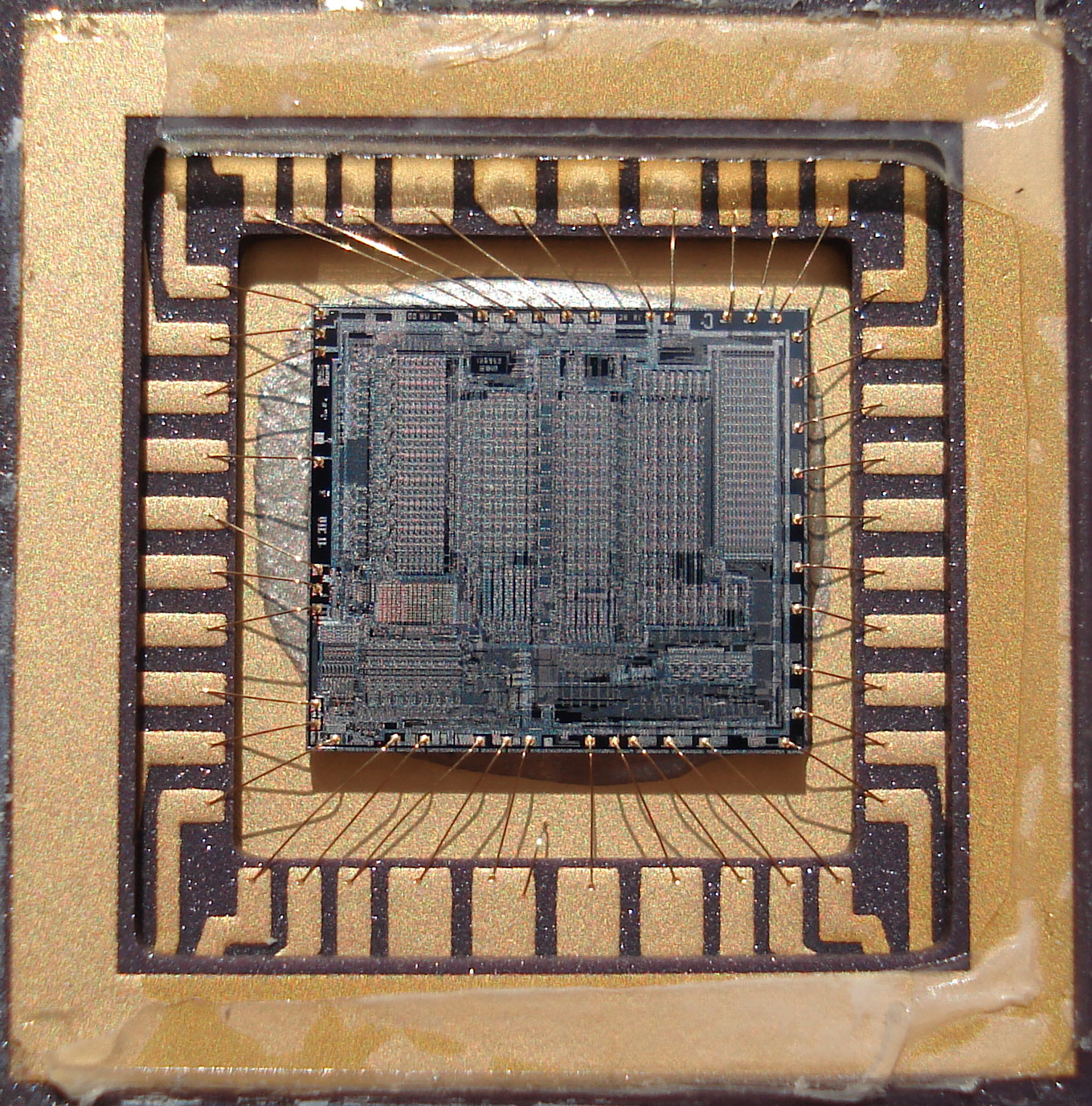
VIC2 6569 R1
VIC2 6569 R3
SID 6581 R2
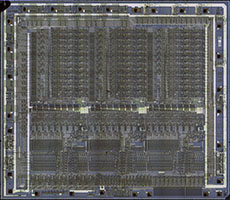
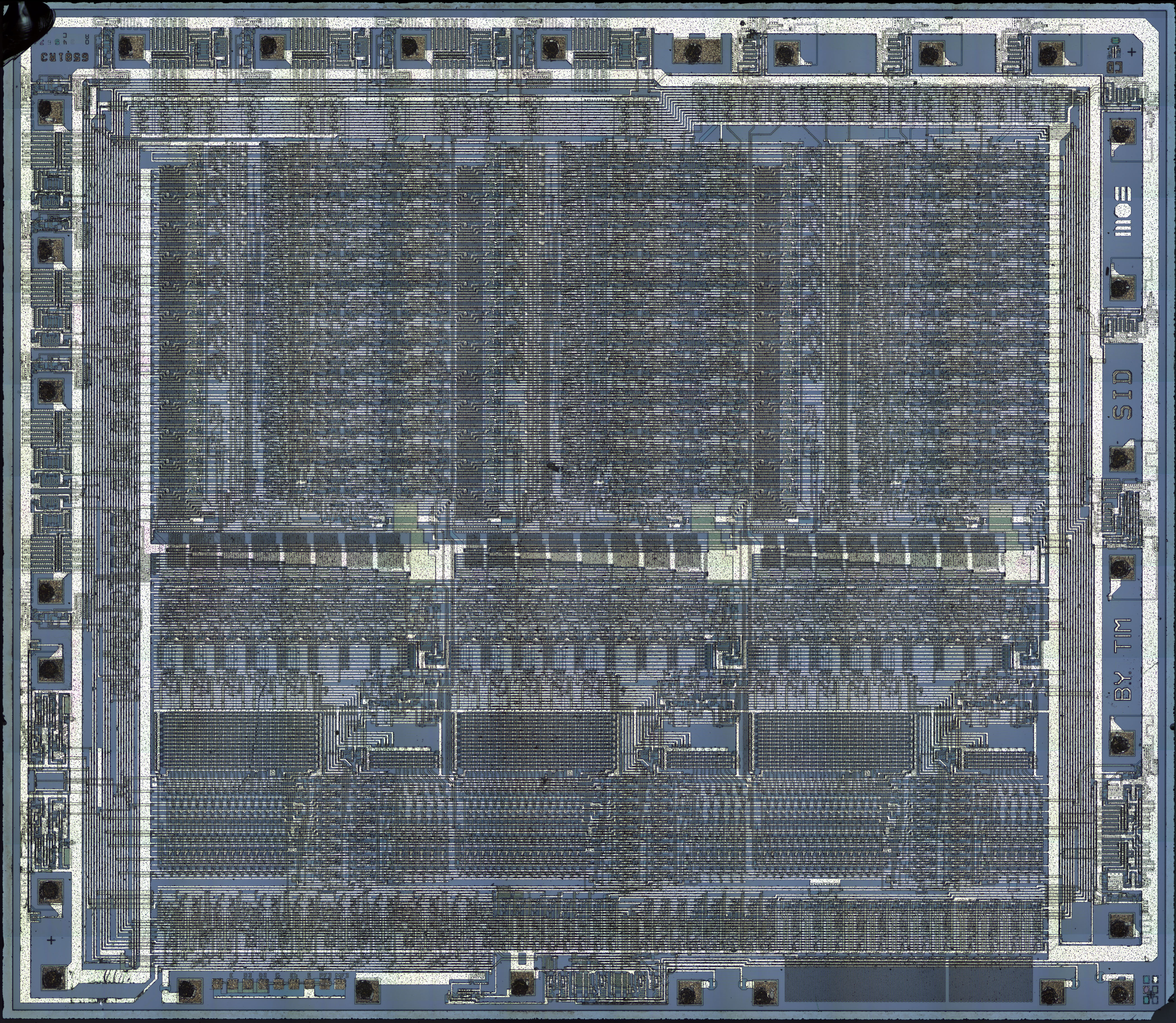
SID 6581 R3
SID 6581 R4
MOS 8580 R5
MOS 8726 R1
Some words:
As of May 2008 I am doing my PhD in surface science (physics) and so I have access to some nice instruments. Also some kind people send me chips that I can do a little testing what method works best to make die shots. After a short investigation under a usual light microscope it turned out that it would be sufficient enough, since the structures are so big. Any method with higher resolution would just increase the preparation efforts and it would be too high resolution to do a mapping of the die in a reasonable time.
So I asked a bit around and our optics group has a very suitable instrument. The microscope is an Axioplan 2 from Zeiss with a software driveable XY-table with micrometer precision and a CCD camera. All images were taken with impinging light.
Darkfield mode means that the lightsource is at an small angle and the microscope optics sees only the diffuse refracted light. So there can be seen edges more pronounced.
Credits:
- support from the optics group, especially Moritz Beleites
- VIC2 dies from Stephan Lesch (ceramic R1 and R3)
- SID 6581 R3 die from Tommi Lempinen aka ZrX-oMs
- SID 6581 R4 die from Jarkko Lehti aka Grue / Beyond Force
- MOS 8580 R5 die from Jarkko Lehti aka Grue / Beyond Force
- MOS 8726 R1 die from Wolfgang Moser
- recordings taken by Michael Huth (that's actually me)
- more credits in the specific die descriptions
Overall die properties and notes:
The chips are NMOS with metal on oxide layer. Under impinging light the metal layer reflects brighter, the different color from lower layers is probably due to interference effects. There might be deeper layers that can not be seen directly. Contacts between the 1st and 3rd layer are probably the small round circles.
The typical width of such metal layer path is 6 micrometers.
Be aware that the focus plane of the microscope at high magnification is very small, so only one layer is really sharp. This is specifically the case for the high magification images of the left part of the SID 6581 filters.
The microscope shows some weak double image reflection in the camera optics path in the Y-direction but this is only noticeable on structureless planes. Don't take these for real.
The nominal magnification is about 1000x for the full die.
Note on the images:
Some are about 20000 by 20000 pixels and won't open in the browser, please save and use a real application.
If your memory gets filled, get a suitable computer.
All the greenish images are not yet auto leveled and auto colored.
So if you would like to have the typical metallic look, auto level and auto color (naming as in photoshop) the images yourself.
VIC II 6569 R3
got this chip from Stephan Lesch
This was the first try, the stepwitdh in Y-direction was taken slightly too high, so there are some micrometers without overlap. Though the image is available.
You can compare to the complete VIC2 6569 R1 die shot for the missing areas. The defect of the R3 is unknown.
VIC2 6569 R3 local marking on the die
VIC2 6569 R3 full die overview, just gray and 25% resolution
VIC2 6569 R3 full die 100% resolution, JPEG highest compression, 29 MB
Full resolution lossless compressed is around 650 MB on ftp.
click thumbnail for full size
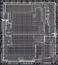
VIC II 6569 R1
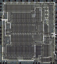
got this one from Stephan Lesch
This was the seconds attempt with a higher overlap. Softwareside defect looks like non-working rasterline counter, maybe someone finds the source of the defect on the die? ;-)
VIC2 6569 R1 full die 100%, JPEG highest compression, 28 MB
cleaned up Version at lower resolution
done by Tommi Lempinen
small image with notes on the function blocks: http://www.mayhem64.co.uk/c64design2.jpg
Also checkout ftp-server for non-rared files.
Lossless compressed TIF of the stitched die:
File 1
File 2
File 3
File 4
File 5
File 6
File 7
File 8
File 9
File 10
File 11
File 12
File 13
File 14
File 15
File 16
File 17
File 18
File 19
File 20
File 21
File 22
File 23
File 24
File 25
File 26
File 27
File 28
File 29
File 30
File 31
File 32
additional re-vectorization work and more stuff at Tommis server:
http://oms.wmhost.com/misc/
It is worth checking this out !
VIC2 6569 R1 darkfield images of certain areas
File 1
File 2
File 3
File 4
File 5
File 6
File 7
File 8
File 9
File 10
Original PNG Images, each file is 20,000,000 Bytes:
Stepwidth in X 0.5 mm and in Y-direction 0.45 mm
File 1
File 2
File 3
File 4
File 5
File 6
File 7
File 8
File 9
File 10
File 11
File 12
File 13
File 14
File 15
File 16
File 17
File 18
File 19
File 20
File 21
File 22
File 23
File 24
File 25
File 26
File 27
File 28
File 29
File 30
File 31
File 32
File 33
File 34
File 35
File 36
File 37
File 38
File 39
File 40
File 41
File 42
File 43
File 44
File 45
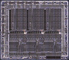
SID 6581 R2
all these images can be found on the ftp-server.
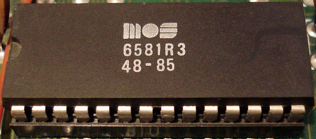
SID 6581 R3
got this die from Tommi Lempinen aka ZrX-oMs
Burnt out of the plastic package. Defect unknown (was it defect before opening?)
Tommi: "Anywho, the process I took to open it was to heat up the stove to the max, then left the chip on it (damn what horrible smell it was). After a bit of smoke I dropped the chip into cold water, then repeated the heating and cooling. Finally took two pliers and cracked open the package, and there was the die."
SID 6581 R3 full die 100% resolution, JPEG highest compression, 22 MB
cleaned up Version at lower resolution,
done by Tommi Lempinen
additional re-vectorization work and more stuff at Tommis server:
http://oms.wmhost.com/misc/
It is worth checking this out ! This is where current development snapshots of partial reverse engineering is posted.
Join #sid on IRCNet to reach people involved.
external links (Everything still in the works):
SIDs function blocks
on chip signal routing
Output and Filter stage as color layers
Filter circuit?
You think something is awfully wrong?
Got some experience with circuity and see the internal working of some function block?
Send a mail.
Full resolution lossless compressed TIFF, each file 20,000,000 bytes:
File 1
File 2
File 3
File 4
File 5
File 6
File 7
File 8
File 9
File 10
File 11
File 12
File 13
File 14
File 15
File 16
File 17
File 18
File 19
File 20
File 21
File 22
File 23
File 24
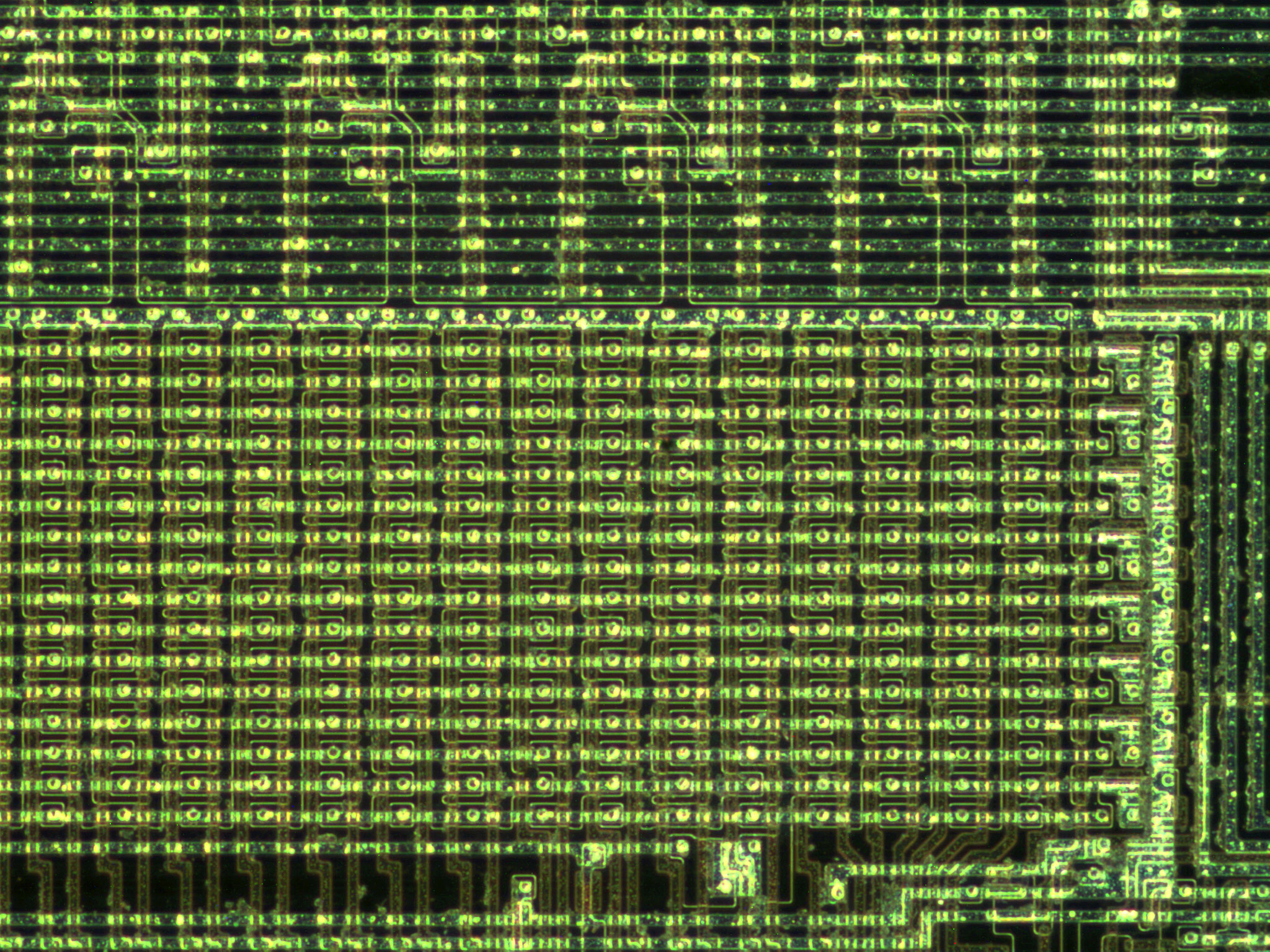
The analog filter circuity seem to have two similar parts. So I imaged the left part in higher resolution.
Focus plane is on the brown layer. This seems to be the limit a normal visible light microscope is capable of.
This area is near the lower right edge of the die.
SID 6581 R3 left half of analog filter at very high resolution. 50% resolution (of the higher resolution), JPEG quality 15%.
This was stitched from about 20 images.
Additional 3 images of the same area with focus plane on the topmost metal layer (JPEG Quality 15%):
SID 6581 R3 detailed analog filter 1
SID 6581 R3 detailed analog filter 2
SID 6581 R3 detailed analog filter 3
These detailed images are taken at a higher resolution and the same area with different focus planes:
Least significant bit of Volume control 1
Least significant bit of Volume control 2
least or most significant bit of resonance control 1
least or most significant bit of resonance control 2
ext-in-to-filter control bit 1
ext-in-to-filter control bit 2
most significant bit of cutoff ? 1
most significant bit of cutoff ? 2
Darkfield images:
SID 6581 R3 output stage, 100% resolution, 30% JPEG quality.
SID 6581 R3 audio amplifier, 100% resolution, 60% JPEG quality.
SID 6581 R3 filter stage, 100% resolution, 60% JPEG quality.
SID 6581 R3 lookup table?, 100% resolution, 60% JPEG quality.
SID 6581 R3 something else?, 100% resolution, 60% JPEG quality.
Original PNG Images, each file is 20,000,000 Bytes:
Stepwidth in X 0.5 mm and in Y-direction 0.42 mm
File 1
File 2
File 3
File 4
File 5
File 6
File 7
File 8
File 9
File 10
File 11
File 12
File 13
File 14
File 15
File 16
File 17
File 18
File 19
File 20
File 21
File 22
File 23
File 24
File 25
File 26
File 27
File 28
File 29
File 30
File 31
File 32
File 33
File 34
File 35
File 36
File 37
File 38
File 39
File 40
File 41
all these images can also be found on the ftp-server.
SID MOS6581 R4AR week 34 year 1988
got this one from Jarkko Lehti aka Grue / Beyond Force
obviously identical die as CSG6581 R4AR Week 37 Year 1989 (also from Grue)
Full size quality 30 die shot JPG
Filter are quality 30 JPG
Logo in high magnification quality 30 JPG
some other filter related circuit quality 30 JPG
Lossless compressed full die (TIF):
File 01
File 02
File 03
File 04
File 05
File 06
File 07
File 08
File 09
File 10
File 11
File 12
File 13
File 14
File 15
File 16
File 17
File 18
File 19
File 20
File 21
File 22
File 23
Original recorded PNG images:
File 01
File 02
File 03
File 04
File 05
File 06
File 07
File 08
File 09
File 10
File 11
File 12
File 13
File 14
File 15
File 16
File 17
File 18
File 19
File 20
File 21
File 22
File 23
File 24
File 25
File 26
File 27
File 28
File 29
File 30
File 31
File 32
File 33
File 34
all these images can also be found on the ftp-server.
Note to the R4AR: The die seems to be nearly identical to the R3, especially in the filter area. Noticeable are the color differences of the oxide layer. The differences are real because the microscope light is calibrated to 3200K. The guess is that the different behaviour of the filter is due to some material change. This could be checked with some micrometer spectroscopy.
SID MOS8580 R5 week 02 year 1988
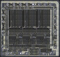
got this one from Jarkko Lehti aka Grue / Beyond Force
obviously identical die as CSG8580 R5 week 05 year 1991 (also from Grue)
Full die image quality 30 JPG
Lossless compressed full die image (TIF):
File 01
File 02
File 03
File 04
File 05
File 06
File 07
File 08
File 09
File 10
File 11
File 12
File 13
File 14
File 15
File 16
File 17
File 18
File 19
File 20
Original recorded PNG images:
File 01
File 02
File 03
File 04
File 05
File 06
File 07
File 08
File 09
File 10
File 11
File 12
File 13
File 14
File 15
File 16
File 17
File 18
File 19
File 20
File 21
File 22
File 23
File 24
File 25
File 26
File 27
all these images can also be found on the ftp-server.
REU Controller MOS 8726 R1
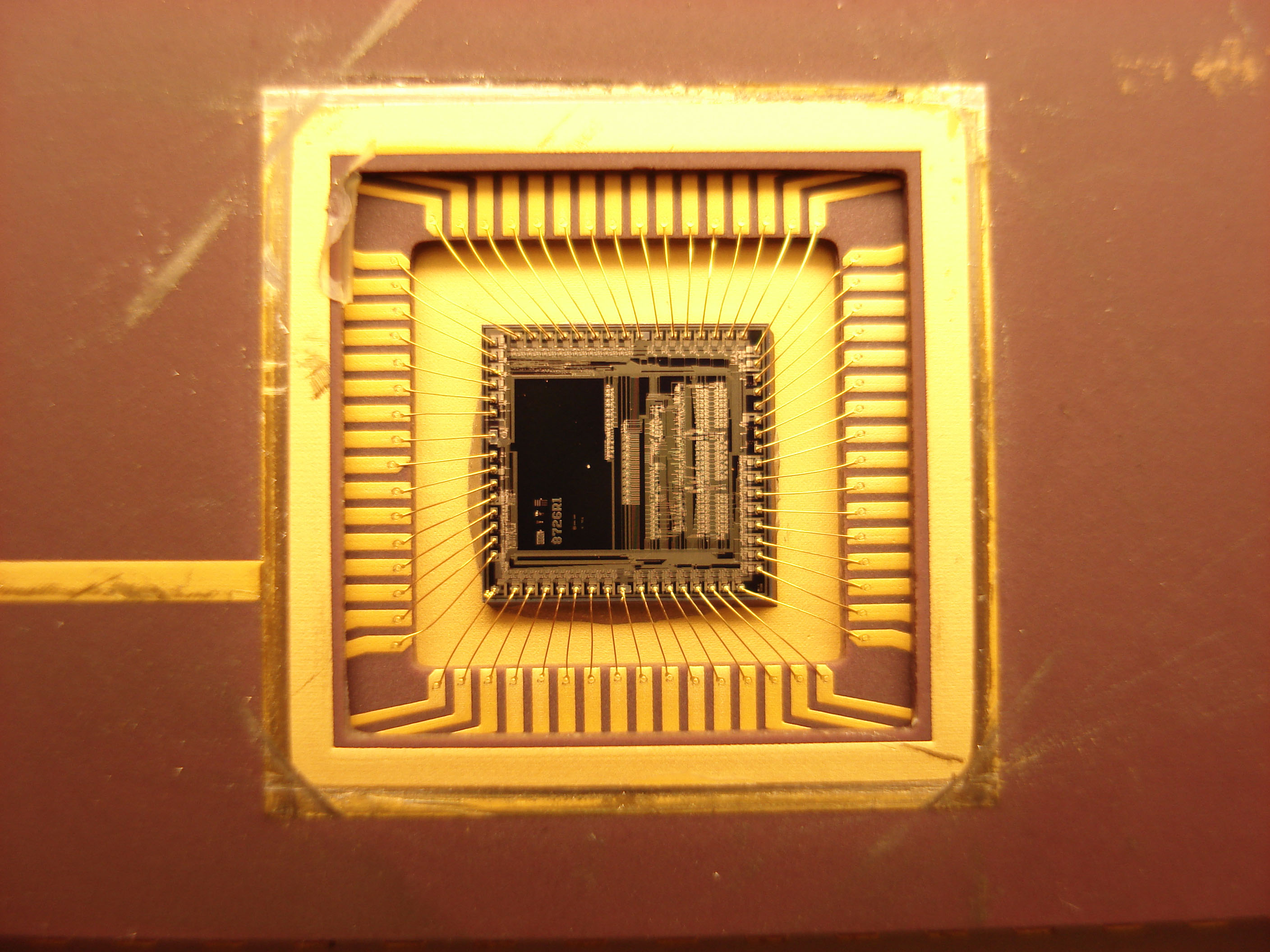
Low quality JPG image full resolution (17826x17063)
original microscope images can be found on the ftp-server.